DARPA’s new Request for Information (RFI DARPA‑SN‑25‑88) on Very Large‑scale Photonic Integration marks a quiet but consequential turn in the U.S. defence approach to quantum hardware. The notice invites industry to propose how photonic integrated circuits (PICs) can scale from today’s tens‑to‑hundreds of components into coherent circuits with thousands—or conceivably millions—of photonic elements suitable for quantum sensing, communications and computing payloads fielded in real systems. In effect, DARPA is asking for a path from lab‑grade PICs to manufacturable, integration‑ready platforms for defence quantum systems.
Key Facts
| Item | Detail |
|---|---|
| RFI Issued | DARPA published VLPI RFI (DARPA‑SN‑25‑88) on 24 June 2025; responses due 15 July 2025. [1][2] |
| Focus | Concepts that move beyond incremental device tweaks to disruptive, Very Large‑scale Photonic Integration pathways. [2] |
| Integration target | Minimise electro‑optical conversions; co‑design photonic and electronic subsystems; enable large‑circuit automation. [1] |
| Related RFI | QuIC PICs (DARPA‑SN‑25‑95) seeks PIC interfaces for quantum emitters (atoms, quantum dots). [3] |
| Industrial support | AIM Photonics test services bolster a domestic PIC ecosystem for defence prototyping. [4] |
Why VLPI matters now
Quantum‑enabled sensing, resilient communications and specialised computing are edging toward deployment. Yet the photonic hardware stack has become a chokepoint: today’s PICs often target isolated functions—modulators, splitters, filters—or topologies with limited scale. Very Large‑scale Photonic Integration reframes the problem as a systems challenge. If defence quantum subsystems are to be rugged, compact and economical, then the photonics must scale like electronics once did—from handmade devices to design‑automated circuits and qualified modules.
This is not simply a call for “more components.” The RFI emphasises manufacturability, yield, packaging and calibration at scale, together with co‑design of photonics and electronics. That co‑design imperative mirrors the historic leap from discrete transistors to VLSI in microelectronics, but with optical phase control, thermal drift and coupling tolerances added to the equation. [1][2]
What DARPA is really asking for
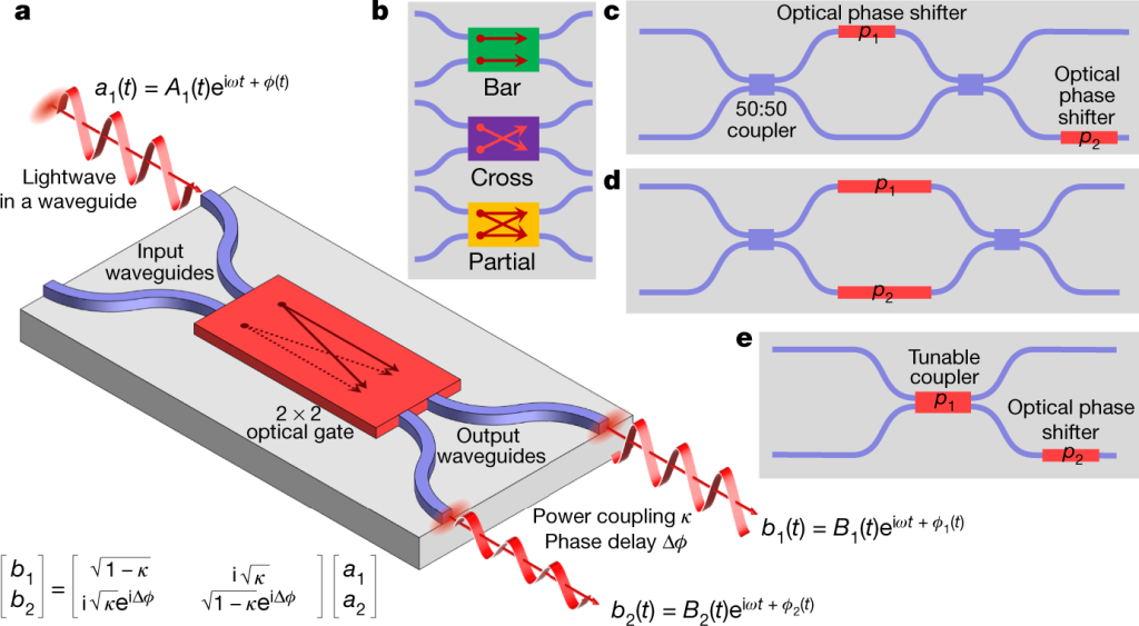
1) Circuit‑class PIC design automation. Handling thousands‑to‑millions of interferometers, phase shifters and couplers demands photonic electronic‑design‑automation (EDA) stacks: parameterised cells, process‑design kits (PDKs), hierarchical layout, timing/phase closure and statistical yield models. Tooling must capture thermo‑optic and electro‑optic behaviours, crosstalk and waveguide dispersion while remaining computationally tractable at circuit scale.
2) Fewer electro‑optical boundaries. Every conversion between electrons and photons adds latency, power and noise. VLPI encourages architectures that push signal routing, filtering, mixing and some compute into purely photonic domains—reserving electrons for control, memory and edge interfaces. This reduces overheads and helps SWaP (size, weight and power) budgets for deployed defence systems.
3) Quantum‑aware interfaces. The companion QuIC PICs RFI homes in on interfaces between PICs and quantum emitters (e.g., neutral atoms, quantum dots). Together, the two RFIs outline an architecture where quantum sensors or repeaters couple to large‑scale photonic backplanes that distribute, process and stabilise quantum‑relevant signals with robust electronics in the loop. [3]
4) Packaging, calibration and reliability at scale. Phase‑stable operation across large meshes requires thermal control, feedback, and stress‑tolerant packaging. Calibration pipelines must scale from wafer sort to module burn‑in, with embedded diagnostics and on‑device heaters/monitors to tame drift through life.
5) Fault‑tolerance and reconfigurability. At large scales, defects are inevitable. Topologies should permit redundancy, rerouting and graceful degradation—akin to network‑on‑chip ideas—so a few dead elements do not doom the circuit. Photonic switching fabrics and reprogrammable meshes can absorb faults without sacrificing mission performance.
Strategic implications for defence programmes
Near‑term contracting signals. An RFI is not a programme of record, but it is a bellwether. Respondents that demonstrate credible Very Large‑scale Photonic Integration roadmaps—tooling, foundry access, packaging flows, quantum interfaces—are well positioned for subsequent BAAs, prototypes and demonstrations under DARPA or service labs. [1]
Ecosystem assembly. No single firm spans all the needed disciplines. Expect consortia linking PIC foundries, design‑tool vendors, quantum hardware teams, packaging houses and test labs. U.S. initiatives like AIM Photonics, with opto‑electronic test services, provide infrastructure to accelerate these collaborations. [4]
Bridging to systems of record. The follow‑through challenge is insertion into real programmes: quantum navigation payloads, secure optical comms, photonic‑assisted EW/radar front‑ends and data‑center‑adjacent accelerators. Here, SWaP‑reliability constraints and MIL‑STD qualification become decisive, as will NATO interoperability profiles once allied co‑development ramps up.
Standards and qualification. Over time, DoD and NATO standards bodies may need to codify photonic circuit classes, interface tolerances, calibration hooks and environmental qualification bands—analogous to how electronics standards (e.g., MIL‑PRF, AEP) matured. Early engagement avoids a future bottleneck when multiple VLPI‑derived modules must interoperate in the field.
Engineering hurdles: what could break
Technological overreach. Scaling PICs is not free. Waveguide loss, heater power, thermal crosstalk and phase noise all accumulate with size. Without novel materials, layout strategies and feedback control, the benefits of Very Large‑scale Photonic Integration could saturate before reaching the desired complexity.
Cost and schedules. Photonic tape‑outs, mask sets, specialised packaging and metrology are expensive. Long fabrication cycles and limited foundry capacity can stretch timelines and limit iteration speed compared to CMOS.
System‑fit risk. If programme managers discover that discrete modules or modestly‑sized PIC tiles meet mission needs with lower risk, some VLPI ambitions may downshift toward modular PIC tiles or photonic network‑on‑chip approaches rather than monolithic giants.
Plausible pathways that balance risk
Hybrid photonic–electronic co‑design. Keep photonics for the functions it does best (ultra‑low‑latency routing, filtering, beamforming, analog multiply‑accumulate), while electronics handles control and digital logic. This keeps the aim of Very Large‑scale Photonic Integration but avoids all‑optical purism.
Tiled meshes with network‑on‑chip concepts. Instead of a single monolith, compose systems from qualified PIC tiles linked by low‑loss couplers or fibre arrays. Each tile is testable and replaceable; the network provides bandwidth and redundancy.
Automation‑first development. Invest in PDK‑anchored EDA early, even for smaller demonstrators. Tooling maturity compounds—reducing respins, tightening tolerances and turning lab insights into reproducible circuit behaviours.
What to watch next
- Follow‑on solicitations: BAAs or SBIRs that convert RFI concepts into funded prototypes and flight‑relevant demos.
- Design‑tool announcements: partnerships between PIC foundries and EDA vendors releasing circuit‑class photonic PDKs.
- Packaging breakthroughs: phase‑stable, low‑power thermal control schemes and calibration‑in‑the‑loop modules.
- Qualification roadmaps: DoD/NATO working groups scoping photonic reliability and interoperability test suites.
For defence and quantum suppliers, the signal is clear: begin assembling cross‑disciplinary teams that can deliver on scaling, integration and qualification. If the hurdles are met, Very Large‑scale Photonic Integration can become a foundational layer across quantum‑enabled defence systems.
Internal links
- Defence Agenda — Quantum & PNT systems (analysis)
- Defence Agenda — Emerging defence microelectronics & photonics (news)
External links
- GovTribe — DARPA SN‑25‑88 VLPI RFI
- Defence Science Institute — DARPA VLPI RFI (full text)
- DARPA — QuIC PICs RFI DARPA‑SN‑25‑95
- Military Aerospace — Very‑large‑scale optical integrated circuit manufacturing
References
- GovTribe — DARPA SN-25-88 VLPI RFI
- https://govtribe.com/opportunity/federal-contract-opportunity/request-for-information-very-large-scale-photonic-integration-vlpi-darpasn2588
- Defence Science Institute — DARPA VLPI RFI (full text, PDF)
- https://defencescienceinstitute.com/wp-content/uploads/2025/06/DARPA-SN-25-88.pdf
- DARPA — QuIC PICs RFI (DARPA-SN-25-95)
- https://www.darpa.mil/work-with-us/opportunities/darpa-sn-25-95
- Military Aerospace — Very-large-scale optical integrated circuit manufacturing
- https://www.militaryaerospace.com/computers/article/55301608/optical-integrated-circuit-computing